
Micron targets 42 Gb/mm2 density for 2027 NAND launch
The company plans to bond two wafers together to double storage capacity and boost speeds by 50 percent.
By Petra Murphy ·
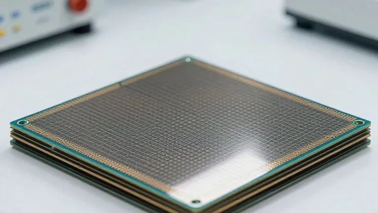
Micron Technology is preparing to double the storage density of its flash memory, a move that hinges on a manufacturing technique it has delayed for years. At an industry event this week, the company detailed its next generation of 3D NAND, designated G11, which is scheduled to begin mass production in the second half of 2027. The new chips are designed to reach a density of approximately 42 Gb/mm2, up from the current G9 generation's 21 Gb/mm2.
The performance gains extend beyond raw capacity. Micron projects that input/output speeds will increase by 50 percent, rising from 3,600 MT/s to 5,400 MT/s. The company also expects the energy required to transfer each bit of data to drop by more than 25 percent. These improvements are intended for high-capacity solid-state drives used in data centers and client devices, as well as newer storage architectures built for artificial intelligence workloads that require high bandwidth and low power consumption.
The technical leap relies on wafer-on-wafer bonding. Instead of fabricating the entire chip on a single wafer, Micron will build the memory array and the peripheral circuitry on separate wafers. Each wafer is processed using the specific technology best suited for its function. The two wafers are then bonded together to form the final component. This approach allows for independent optimization of the memory cells and the logic circuits, a capability that previous CMOS-under-array designs did not fully provide.
Scott DeBoer, Micron's president and chief technology and products officer, stated that the company had previously promised to adopt this technology when it became cost-effective. "This is the right timing for that technology," DeBoer said. He described G11 as the world's most advanced NAND and confirmed that the design is based on wafer-on-wafer bonding, a method already employed by Chinese competitor YMTC.
G11 will also exceed 400 active wordline layers, although Micron has not disclosed the exact count. The company attributes the density jump to a combination of increased layer counts and a reduction in memory cell pitch. DeBoer noted that the industry continues to scale by adding layers and shrinking cell dimensions. He added that Micron is developing new high-mobility materials and ultra-dense cell architectures to support future generations beyond G11.
Micron has not released specific technical details or production schedules for generations following G11. The company plans to share more information in 2027, closer to the start of high-volume production. For now, the 42 Gb/mm2 target stands as a measurable increase over the next-generation products currently planned by rivals Kioxia and Samsung.